- cross-posted to:
- hardware@lemmy.world
- cross-posted to:
- hardware@lemmy.world
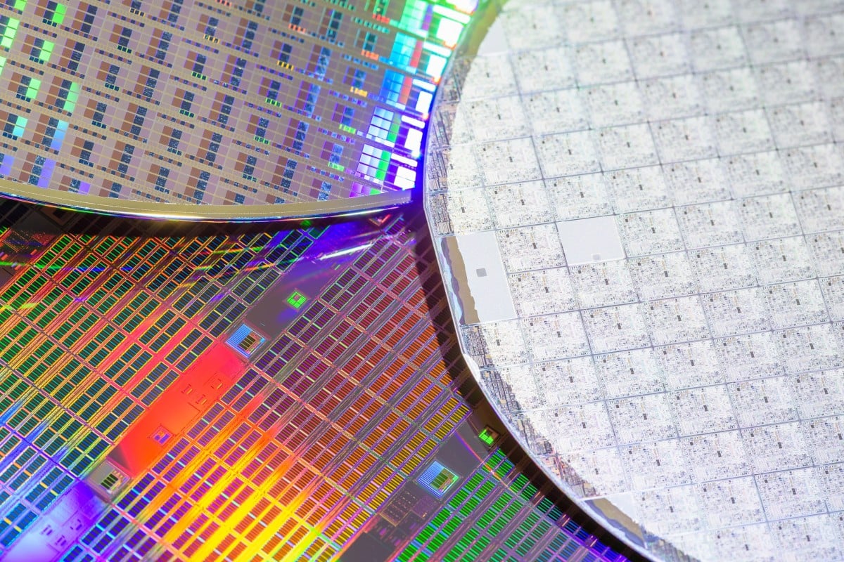
Beijing is set to spend 33 billion yuan (US$4.6 billion) building a 12-inch wafer fabrication facility, led by state-owned enterprises and funds, marking another step in China’s efforts to boost domestic semiconductor production.
Leading firms involved in the new facility include Beijing Yandong Microelectronics (YDME), which is listed on Shanghai’s Star Market, and BOE Technology, China’s top display maker.
This year, companies including Huahong Semiconductor, China Resources Microelectronics, and Guangzhou ZenSemi have all announced progress on 12-inch wafer fabs.
Meanwhile, Semiconductor Manufacturing International Corporation, which established the mainland’s first 12-inch foundry in 2004, reported full utilisation of its 12-inch capacity in the third quarter. Revenue from 12-inch wafers accounted for 78.5 per cent of its 15.6 billion yuan total for the quarter. The company expects to release an additional 30,000 wafers per month in the fourth quarter.
Recently, Chinese chip design firms have become concerned that Taiwan Semiconductor Manufacturing Company, the world’s leading contract chipmaker, might suspend 7-nanometre node services for certain AI chip clients due to mounting pressure from the US. The Taiwanese chipmaker recently told mainland clients that it would no longer accept orders from them for advanced chips after TSMC technology was found in a product from US-sanctioned Huawei Technologies.


Cyberspace will be beautiful again one day. Datacenters, undersea cables, and nuclear reactors for EVERYONE! EVERYONE!