
- cross-posted to:
- nvidia@lemmy.world
- cross-posted to:
- nvidia@lemmy.world
You must log in or register to comment.
This is the best summary I could come up with:
With today’s debut of the Blackwell GPU architecture during CEO Jensen Huang’s GTC keynote, it aims to extended that lead — in both performance and power consumption.
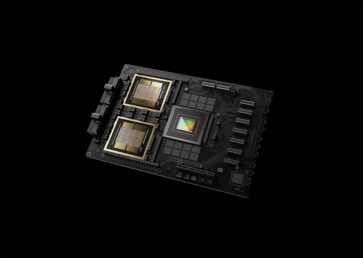
AMD’s MI300-series accelerators, which we looked at in December, are objectively more complex and rely on both 2.5D and 3D packaging tech to stitch together as many as 13 chiplets into a single part.
This means if your datacenter can already handle Nvidia’s DGX H100 systems, you shouldn’t run into trouble adding a couple B100 nodes to your cluster.
However, considering the fact that the older GH200 was rated for 1,000W between an 700W and the Arm CPU, that suggests that, under peak load, the Grace-Blackwell part, with its twin GPUs is capable of sucking down somewhere in the neighborhood of 2,700W.
Nvidia’s rackscale architecture appears to be a hit with the major cloud providers too, with Amazon, Microsoft, Google, and Oracle signing up to deploy instances based on the design.
As we mentioned earlier, the MI300X is something of a silicon sandwich which uses advanced packaging to vertically stack eight CDNA 3 compute units onto four I/O dies, which provide high speed communications between the GPUs and 192GB of HBM3 memory.
The original article contains 1,849 words, the summary contains 199 words. Saved 89%. I’m a bot and I’m open source!