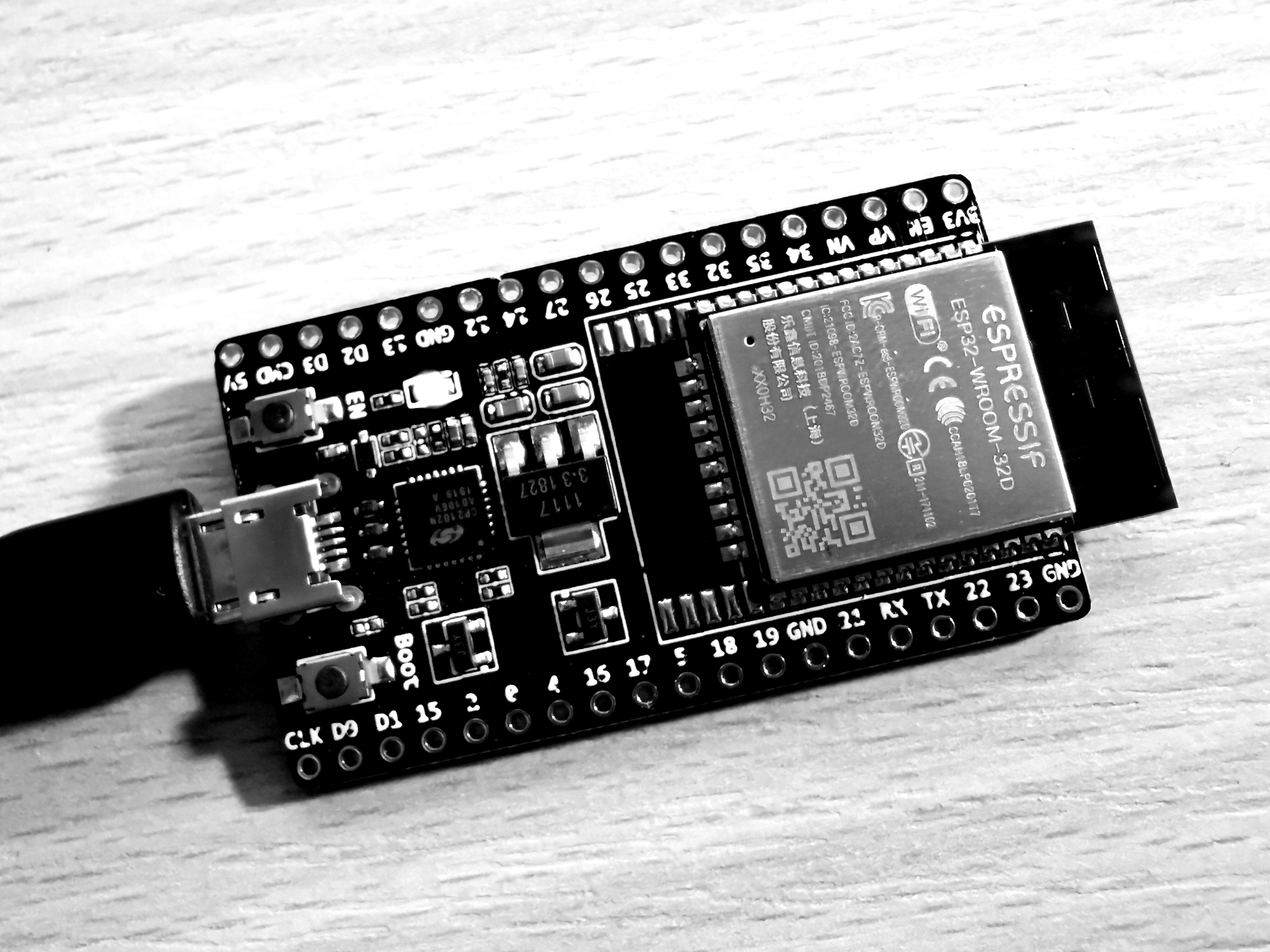
I am not much of an EE and I was wondering if there is a place where I can find schematics of popular esp32 dev boards? My hope is that I can do placement and wire routing on a known good schematic. I know that PDF version of the schematic is available and technically it is possible to recreate it in KiCad but I’m hoping to find something in native KiCad format so that I have a good starting point for making custom board shapes.


Few things to consider, you should have decoupling caps near the esp32s vcc and these need to be as close to it as possible. The antenna should be off the pcb completely and have gaps on its side, the module shouldn’t be in the middle of the board for instance.
I think the new modules can be connected directly from usb and don’t need uart, something to look into.
Tbh though, if it’s to learn, I would make an arduino first. The atmega chip comes in a dip format so you can make the whole thing on bread board first.
A good ressource is the printedcircuitboards sub on reddit. They won’t have kicad projects but will have vaste amounts of schematics that you can study and copy with comments outlining mistakes and things of that nature.
Thanks. These tips help a lot.
I wouldn’t say that the goal is to learn. I have implemented the design on a Dev board. I also designed a breakout board which worked well. I am now considering just trying to do a new layout in a smaller form factor.
There are bigger system integration tasks that I need to address before I can spend my resources on learning ESP32’s board layout. That is why I wanted to derisk my design by building on top of a known good design or at least find out the best practices of board layout.
Here’s the official schematic for the module. It’s from the esp32 hardware reference in the official docs, under devkitc v4
https://dl.espressif.com/dl/schematics/esp32_devkitc_v4-sch-20180607a.pdf
Probably your best bet!
Thanks!